
Background
III-V semiconductors are the preferred choice for RF, Power and space/ defense applications. Though expensive, they offer many advantages over silicon like higher power handling capacity, break down voltage etc.

Fig.1 Typical HEMT structure with 2DEG at AlGaN/GaN interface[1]
We are familiar with the concept of two-dimensional electron gas(2DEG) in III-V semiconductors which form the basis of High Electron Mobility Transistor(HEMT).
The 2DEG is created due to a triangular quantum well formation at the heterojunction(between semiconductor materials) causing quantum confinement[3][4].

Fig.2 Typical HEMT structure with 2DE G at AlGaN/GaN interface[2]
As ionized impurities are absent(to induce electrons), the scattering is minimal, leading to higher mobility(hence current) versus Si-based devices.The electron density in case of III-Nitride 2DEG is about ∼5 × 1013 cm−2.
In 2004, the turf of III-V semiconductors was challenged when researchers found the presence of high-density 2DEG at an oxide interface(LaAlO3 & SrTiO3) which exceeded the values seen in III-Nitride 2DEG[5][6]. Similarly, GdTiO3-SrTiO3 heterostructure grown on an oxide substrate has demonstrated 2DEG electron density >3 × 1014 cm−2 [5][7]. Devices based on these oxides have the potential of being used as sensors, Field Effect Transistors(FETs) etc.

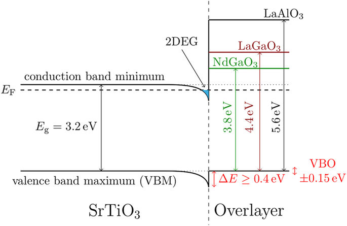
Fig.3 Band diagram of STO-LAO interface with 2DEG[6][11]
The only hindrance to realizing the full potential of oxides for Optronics application is the current use of single crystal oxide substrates for material/film growth[5].
For commercial viability, we would like to use single crystal substrates like silicon(001) or (111) with some demonstrations already being made for adoption[8][9][10]
- LTO-STO heterostructure on Si(100) with a 2DEG charge density of 8.9 × 1014 cm−2
- GdTiO3-SrTiO3 on Si(001) with a 2DEG charge density of ∼9 × 1013 cm−2
Taking another step in this direction, researchers at Yale University have added a new substrate for the growth of oxides – GaAs(III-V material)[5]. They have been able to grow GdTiO3-SrTiO3 heterostructure on GaAs wafer using MBE. The electron density obtained at the GTO–STO interface is ∼2 × 1014 cm−2 [5].
Article
Further Reading
In the future, post optimization and scaling, the devices fabricated on these films can act as the baseline for the next-generation electronic and optical devices.
If you want to share your opinion kindly do so in the comments section or email me at u2d2tech@gmail.com.
References:
- http://www.semiconductor-today.com/news_items/2010/APRIL/UCSB_150410.htm
- M. Aadit et. al, “High Electron Mobility Transistors: Performance Analysis, Research Trend and Applications, Different Types of Field-Effect Transistors – Theory and Applications”, InTech, 10.5772/67796, 2017
- https://en.wikipedia.org/wiki/Two-dimensional_electron_gas
- http://uef.fei.stuba.sk/moodle/mod/book/view.php?id=7920&chapterid=63
-
L. Kornblum et. al.,”Oxide heterostructures for high-density 2D electron gases on GaAs”, Journal of Applied Physics,123,025302,2018 - A. Ohtomo et. al.,”A high-mobility electron gas at the LaAlO3/SrTiO3 heterointerface”, Nature volume427, pages423–426, 29 January 2004
-
P.Moetakef et. al.,”Transport in ferromagnetic GdTiO3/SrTiO3 heterostructures”, Appl. Phys. Lett. 98, 112110, 2011
-
E. Jin et.al.,”A high density two-dimensional electron gas in an oxide heterostructure on Si (001)”, APL Materials 2, 116109, 2014
- L. Kornblum et. al.”Oxide 2D electron gases as a route for high carrier densities on (001) Si”, Appl. Phys. Lett. 106, 201602,2015
- L. Kornblum et. al. “Electronic transport of titanate heterostructures and their potential as channels on (001) Si”, Journal of Applied Physics 118, 105301, 2015
- https://en.wikipedia.org/wiki/Lanthanum_aluminate-strontium_titanate_interface
-
U. Treske et. al., “Universal electronic structure of polar oxide heterointerfaces”, Scientific Reports volume5, Article number: 14506, 2015
- M Lorenz et al,”The 2016 oxide electronic materials and oxide interfaces roadmap”, Physics D: Applied Physics 49,43,2016
- J.H. Yoon et. al, “Electronic Band Alignment at Complex Oxide Interfaces Measured by Scanning Photocurrent Microscopy”, Scientific Reports 7, Article number: 3824 (2017)
- https://www.synchrotron-soleil.fr/en/news/universal-fabrication-two-dimensional-electron-gases-functional-oxides-future-applications
-
Changjian Li et. al, “Tailoring the Two Dimensional Electron Gas at Polar ABO3/SrTiO3 Interfaces for Oxide Electronics”, Scientific Reports 5, Article number: 13314 (2015)
- https://www2.physics.ox.ac.uk/research/oxide-electronics

Fantastic site you have here but I was wondering if you knew of any forums that cover the same topics talked about in this article? I’d really love to be a part of community where I can get opinions from other knowledgeable individuals that share the same interest. If you have any recommendations, please let me know. Bless you!
thank you for sharing with us, I think this website truly stands out : D.
This is the right blog for anyone who really wants to find out about this topic. You realize a whole lot its almost hard to argue with you (not that I actually would want to…HaHa). You definitely put a brand new spin on a topic which has been discussed for many years. Excellent stuff, just excellent!