
Introduction
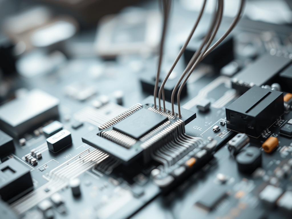
Chip packaging, also known as semiconductor packaging, is the process of enclosing a tiny, delicate semiconductor chip—often called a “die”—in a protective casing that allows it to function reliably in electronic devices.
This final step in chip manufacturing is crucial for both protecting the chip and enabling it to connect with the outside world.
Key Points About Chip Packaging
- Protection: The package shields the semiconductor chip from physical damage, moisture, dust, and corrosion, ensuring long-term reliability
- Electrical Connections: It provides the necessary connections between the chip and the circuit board, allowing signals and power to flow in and out of the chip
- Thermal Management: Many packages help dissipate heat generated during operation, which is critical for performance and longevity
- Miniaturisation: Advanced packaging techniques allow for smaller, more powerful devices by integrating multiple chips or stacking them in three dimensions
How Does Chip Packaging Work?
- Dicing: The silicon wafer is sliced into individual chips.
- Mounting: Each chip is attached to a frame or substrate that supports it and provides pathways for electrical signals43.
- Wire Bonding or Flip-Chip: Tiny wires or bumps connect the chip to the package leads or substrate, enabling electrical communication
- Encapsulation: The chip is sealed in a protective material, such as plastic, ceramic, or metal, to guard against environmental hazards
Types of Chip Packaging
- Traditional: Includes wire-bonded packages, ceramic, and plastic packages
- Advanced: Includes flip-chip, ball grid array (BGA), chip-scale packages (CSP), and wafer-level packaging—each offering improved performance, size, and integration
Why Is Chip Packaging Important?
- It ensures chips can survive handling, assembly, and operation in various environments
- Packaging affects the chip’s performance, power consumption, and the overall size of electronic devices
- As technology advances, packaging is becoming a central innovation point, enabling new applications like AI, IoT, and compact mobile devices
Summary
Chip packaging is more than just “wrapping up” a chip—it is a sophisticated process that determines how well a chip functions, how long it lasts, and how it fits into the ever-shrinking world of modern electronics.
As devices get smaller and more powerful, the importance of advanced chip packaging continues to grow.
References
- https://resources.pcb.cadence.com/blog/2023-semiconductor-chip-packaging
- https://semiengineering.com/knowledge_centers/packaging/
- https://anysilicon.com/the-ultimate-guide-to-semiconductor-packaging/
- https://www.youtube.com/watch?v=7gg2eVVayA4
- https://www.youtube.com/watch?v=IkGdU5ZPDMs
- https://www.bcg.com/publications/2024/advanced-packaging-is-reshaping-the-chip-industry
- https://www.semiconductors.org/wp-content/uploads/2018/06/Whitepaper-on-Semiconductor-Die-and-Packaging-for-SD-AO-May-14-2013.pdf
- https://resources.pcb.cadence.com/blog/2023-semiconductor-packaging
- https://pcbmake.com/chip-packaging/
- https://semiengineering.com/making-chip-packaging-simpler/
- https://news.skhynix.com/semiconductor-back-end-process-episode-2-semiconductor-packaging/
- https://en.wikipedia.org/wiki/Integrated_circuit_packaging
- https://research.ibm.com/blog/what-is-computer-chip-packaging
- https://www.semiconductorreview.com/news/a-guide-to-semiconductor-packaging-nwid-589.html
- https://www.csis.org/blogs/perspectives-innovation/chips-and-semiconductor-packaging
- https://www.polymersolutions.com/the-science-behind-packaging-the-chip-challenge-flavors/
- https://www.semiconductorpackagingnews.com
- https://www.sciencedirect.com/science/article/pii/S2667325823001334

Wow Sir, Thank you 🙂
LikeLiked by 1 person