

Introduction
A CMOS backplane is the active “driving” substrate found behind modern flat-panel and microdisplay technologies. Built using standard Complementary Metal-Oxide-Semiconductor (CMOS) processes, it contains the tiny transistors, capacitors, and interconnects that switch each pixel or sensor element on and off.
Here is a concise look at what it does, where it is used, and the hurdles designers face when integrating it into finished products.
What Is a CMOS Backplane?
- Active Matrix Driver: Each pixel (or sensing element) is paired with one or more CMOS transistors that control its on/off state or readout.
- Built on CMOS Wafer: Leverages mature silicon-fab processes, enabling tight transistor density, low power, and high reliability
- Versatile Interface: Provides digital or analog signals to downstream layers—whether an OLED emissive stack, microLED chips, or photodiodes
Key Applications
- Flat-Panel Displays (OLED, LCD, MicroLED)
- High-resolution televisions, monitors, smartphones, and tablets
- Wearable displays and head-mounted AR/VR optics
- Imaging Sensors & Machine Vision
- CMOS image sensors in digital cameras and smartphones
- LIDAR arrays and IR sensors for automotive and industrial use
- Microdisplays & Near-Eye Systems
- AR glasses, VR headsets, and viewfinders for cameras
- Helmet-mounted displays in aviation and defence
- Fingerprint & Biometric Sensors
- Under-display fingerprint readers in smartphones
- Medical diagnostics chips for lab-on-a-chip systems
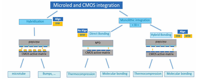
Integration Challenges
- Material Compatibility:
- High-temperature CMOS processes vs. temperature-sensitive OLED or microLED materials
- Stress mismatches can cause layer delamination or pixel defects
- Yield & Defect Management:
- Millions of transistors per backplane—each defect can knock out an entire pixel
- Rigorous testing and redundancy schemes add cost and complexity
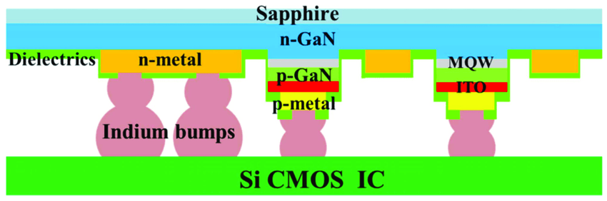
- Fine-Pitch Interconnects:
- MicroLED or OLED pixels must align to CMOS pads with micron-level accuracy
- Flip-chip bonding or micro-transfer printing demands precise alignment and uniform pressure
- Thermal & Power Constraints:
- Dense transistor arrays generate heat, and limited thermal conductivity through stacked layers
- Need for low-power drive schemes to avoid uneven heating (which degrades lifetime)
- Scaling to Higher Resolutions:
- Smaller pixels require thinner gate oxides and tighter lithography, pushing CMOS fabs to their limits
- Increased data rates for video drive higher-speed drivers, raising electromagnetic-compatibility concerns
Looking Ahead
Advances in heterogeneous integration—such as wafer-scale microLED transfer, advanced packaging, and flexible CMOS processes—are steadily addressing these challenges.
As backplane technologies mature, we can expect even sharper, brighter, more power-efficient displays and sensors in everything from our smartphones to our cars and beyond.
Summary
The CMOS backplane is the unsung hero behind today’s high-resolution displays and sensors. While integrating silicon-based drivers with delicate emissive or sensing materials poses real engineering hurdles, ongoing innovations in process integration and packaging are unlocking ever more impressive visual and imaging capabilities.

Leave a comment