
Introduction
As our world becomes increasingly interconnected through 5G networks, satellite communications, and high-performance electric vehicles, the demand for “smaller, faster, and cooler” electronics has never been higher. Standard silicon-based transistors are hitting their physical limits.
Enter the GaN-on-Diamond HEMT, a breakthrough semiconductor technology poised to redefine the boundaries of high-power electronics.
What It Is
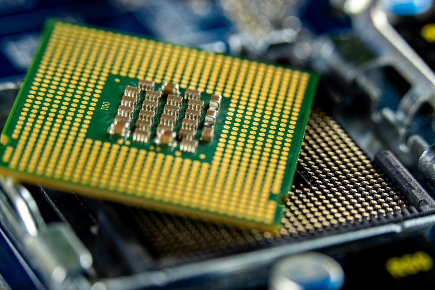
A High Electron Mobility Transistor (HEMT) is a field-effect transistor that utilizes a junction between two materials with different band gaps.
While Gallium Nitride (GaN) has been the industry standard for high-frequency applications, GaN-on-Diamond technology involves replacing the traditional silicon or silicon carbide substrate with synthetic diamond. This creates a heterostructure where the high-speed electrical properties of GaN are merged with the extreme physical properties of diamond.
Why It Is Preferred
The primary reason for this pairing is thermal management. Diamond is the most thermally conductive material known to man – roughly five times more conductive than copper.
In high-power applications, transistors generate immense heat; if this heat isn’t dissipated, performance drops, and the device may fail. By placing GaN directly on diamond, we can:
- Achieve power densities 3 to 10 times higher than GaN-on-SiC.
- Drastically reduce the size of cooling systems.
- Maintain high electron mobility even under extreme stress.
What Are the Challenges?
Despite its promise, the technology is difficult to master.
The biggest hurdle is the lattice mismatch and the coefficient of thermal expansion between GaN and diamond, which can cause the material to crack or peel during manufacturing. Furthermore, creating a high-quality “thermal interface” between the two layers is technically complex and, for now, significantly more expensive than traditional methods.
What to Look Forward To
The horizon is bright.
Research is currently focused on refining “wafer-bonding” techniques to lower costs and improve reliability. As manufacturing scales, expect GaN-on-Diamond to become the backbone of 6G infrastructure, advanced radar systems, and ultra-compact power converters for aerospace. We are moving toward a future where “overheating” is no longer a design constraint.

Leave a comment