

Background
Panasonic Corporation declared that they have been able to develop GaN-based power transistors which exhibit no hysteresis at the threshold voltage[1]. These transistors were processed using films grown on Silicon wafers ie. GaN on Si[1][5].
So why is this development noteworthy??
Let us delve more into this topic……
Basics
Threshold voltage: It is the gate voltage(Vg) beyond which the current starts flowing in the transistor from the source to the drain. This gate voltage(Vg) when plotted in relation to the drain current(Id) shows a shift when repeated measurements are made. This is called as ‘hysteresis’.

Fig 1. Hysteresis in devices with various gate oxides[6]
Hysteresis is induced due to electron traps within the gate insulator which leads to instability in the device[1][4].
To overcome this problem, Panasonic used some novel methodology like
- aluminum oxynitride(AlON) dielectric and
- recessed gate for Normally OFF(NO) operation
Let us talk more about them……..
Breakthrough
Dielectric AlON
Aluminum Oxynitride(AlON) is an insulating material composed of aluminum (Al), oxygen (O), and nitrogen (N). In bulk form, it is known as ‘Transparent Aluminum'[8].
Dielectric films used as gate insulation have some defects leading to electron trapping and modification of Id-Vg curve due to hysteresis.

Fig 2. Traps in gate dielectric[11]
According to Panasonic, Aluminum Oxynitride(AlON), when used as a gate dielectric, does not trap electrons within the film thereby reducing the chances of hysteresis[1][3][4].
Recessed Gate
AlGaN/GaN are Normally ON devices and need to be pinched off using negative voltage(D-Mode).

Fig 3. Id-Vg characteristics for E-Mode and D-Mode FET[9]
Another approach that has been used is recessing(to make E-Mode devices). The thickness of the nitride is modified and a dielectric is grown in the recess followed by metal deposition.

Fig 4. Recessed and Dielectric insulated HEMT[12]
This oxide deposition leads to modification of the band diagram such that the device becomes Normally OFF giving a positive threshold voltage[1][4][13].

Fig 5. Band diagram of MIS-HEMT(E-Mode) v/s HEMT(D-Mode)[13]
The final device structure in comparison the baseline has been shown below. This device structure after achieving suitable yield will hit the production line for ramp up.
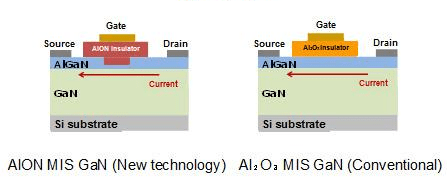
Fig 6. Device structure by Panasonic vs Conventional[1]
Article
http://news.panasonic.com/global/press/data/2018/02/en180223-2/en180223-2.html
Conclusion
With the introduction of a low hysteresis AlON dielectric based devices, Panasonic has paved the way for high-speed switching devices. With reliability now becoming a norm, GaN-based components can be adopted faster leading to substantial savings(energy and financial).
If you want to share your opinion kindly do so in the comments section or email me at u2d2tech@gmail.com.
References:
- http://news.panasonic.com/global/press/data/2018/02/en180223-2/en180223-2.html
- http://news.panasonic.com/global/press/data/2018/02/en180223-2/en180223-2.html#2
- https://compoundsemiconductor.net/article/103586/Panasonic_Develops_Insulated-Gate_GaN_Power_Transistor
- https://www.aninews.in/news/tech/others/panasonic-develops-insulated-gate-gan-power-transistor201802231534190001/\
- https://eu.industrial.panasonic.com/products/semiconductors/power/gan-power-transistors#x-gan-struct
- N. Ramanan et.al., “ALD gate dielectrics for improved threshold voltage stability in AlGaN/GaN MOS-HFETs for power applications”, , ,
- http://www.dtic.mil/dtic/tr/fulltext/u2/a184753.pdf
- http://www.surmet.com/technology/alon-optical-ceramics/index.php
- http://article.sapub.org/10.5923.j.eee.20120205.11.html
- https://phys.org/news/2010-10-fujitsu-gan-hemt-power-amplifier.html
- T. Wu et.al.,”Correlation of interface states/border traps and threshold voltage shift on AlGaN/GaN metal-insulator-semiconductor high-electron-mobility transistors”, Appl. Phys. Lett. ,107, 093507, 2015
- http://www.semiconductor-today.com/news_items/2011/FEB/CREST_100211.htm
- A. Suria et.al.,” DC characteristics of ALD-grown Al2O3/AlGaN/GaN MIS-HEMTs and HEMTs at 600 °C in air”, , ,
- https://www.actuia.com/actualite/panasonic-1000-ingenieurs-intelligence-artificielle-relancer-groupe/

Simply wanna state that this is handy, Thanks for taking your time to write this.
LikeLike