Background
We are very familiar with the concept of miniature display through our smartphones, smartwatches, tablets, e-readers, etc. These displays have undergone a steady evolution through the years starting from Liquid Crystal Display(LCD) to LED Backlight to Active Matrix Organic LED(AMOLED) Display.
The next big development in this area is going to be – Flexible Display
Flexible Display is amenable to being folded/bent as opposed to traditional displays. This is possible due to the organic materials used in making these displays.
Despite being amenable by nature, organic materials have lower reliability and cannot be processed at higher temperatures[5][6][7].
This lacuna can only be overcome if we could
- Increase the reliability of organic materials (work in progress) or
- Use of inorganic materials to make Flexible Display
The possible use of inorganic materials warrants a hybrid heterostructure grown on two-dimensional (2D) layered materials like Graphene or hexagonal Boron Nitride(hBN)[2][18][19][20].
Accordingly, the article talks about the research carried out by two different groups using graphene as the template for GaN growth
In 2014, a research group at Seoul National University (SNU) grew Gallium nitride(GaN) on graphene using MOCVD paving the way for its adoption in Flexible Displays[1][8].
Similarly, in 2017, a Japanese research group grew crystalline GaN films using graphene buffer on an amorphous substrate(glass) with the use of Pulsed Sputtering Deposition (PSD)[2].
Material Characteristics
Graphene is a monolayer of carbon atoms arranged in a chicken wire or hexagonal pattern[1][9].

Graphite(3D) is formed by stacking graphene(2D) which are bonded by weak Van der Waal’s force. A monolayer of graphene was isolated from Graphite in 2004 at the University of Manchester by mechanical exfoliation.

III-Nitride Semiconductors like GaN and InN are used for making Light Emitting Diodes(LEDs) (along with quantum structures like quantum wells, quantum dots, etc.) for covering the entire Visible, Infrared(IR) and UltraViolet(UV) spectrum.
Research is also ongoing to make high-power, deep Ultra-Violet(DUV) LEDs using AlGaN or AlN which have applications in disinfection, curing, gas sensing, and sterilization[21][22][24].
Due to the unavailability of lattice-matched substrates, Nitrides are grown on non-native materials like Sapphire or Silicon Carbide(SiC)[12]. This leads to mismatch and generation of faults like stacking fault, threading dislocation(TDD) etc. at the boundary of GaN/substrate.
When devices are fabricated on these materials, the faults act as trap sites(for the charge carriers) thereby reducing the output and reliability of the LED[15].
Hence the best option is to grow GaN on materials that are lattice matched to it or have a low mismatch to it. This helps in adopting GaN for applications like flexible displays and devices beyond two terminals like HEMT etc.
III-Nitride for Flexible Display??
Organic materials used in fabricating OLEDs are a choice for making flexible displays. III-Nitride materials owing to their superior light output, ease of fabrication,n, and reliability can be adopted to make flexible displays if they meet the following criteria:
- Low-temperature growth
- Compatible with low-cost substrates like plastic, glass, etc.
Normally, III-Nitride semiconductors like GaN, AlGaN, InGaN, etc. are grown using Metal Organic Chemical Vapor Deposition(MOCVD) or Molecular Beam Epitaxy(MBE). Owing to this, the temperature required for a high-quality epitaxial film is more than 850oC [1][2][8].
Also, the substrate(sapphire/SiC) currently utilized for III-Nitride semiconductor growth is crystalline and hence resists any change in shape.
Hence, the substrate of choice should have low lattice mismatch, a similar structure, and be flexible(bendable) for III-Nitride semiconductor growth.
Considering this, one well-researched material meets the criteria – Graphene
Graphene for III-Nitride Growth
As discussed earlier, we are now going to delve into the research work by two groups on their efforts to grow GaN on graphene. The device outcome from the films is similar to GaN on Sapphire or GaN on Silicon Carbide(SiC).
A] Research at Seoul National University(SNU)[2014]
A research group at Seoul National University (SNU) grew Gallium nitride(GaN) on graphene using MOCVD[1][8]. Post-growth, they incorporated a transfer technique that assisted in measuring GaN LEDs on an organic(polyimide) substrate.
- Graphene Growth
Graphene films are grown on Cu foil using Chemical Vapor Deposition(CVD). The grown films are Multi-Layer Graphene(MLG) which is semi-transparent in nature[8].
- Transfer & Growth
This MLG graphene film is then transferred to a SiO2/Si substrate to act as a template for III-Nitride growth.
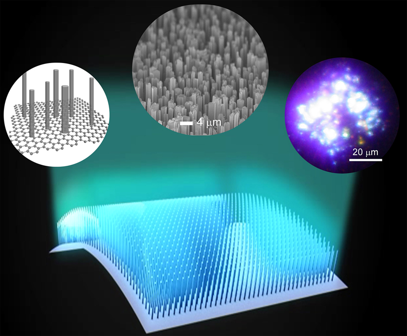
To grow the GaN micro-rods, MOCVD reactants were used along with nitrogen as the carrier gas. A 2-μm-thick GaN buffer layer was grown to improve the vertical alignment of the micro-rods.
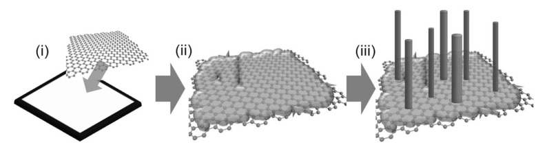
The micro-rods were not grown selectively. The geometry of the GaN micro-rods depends on the growth time[8].
- Material Characterization
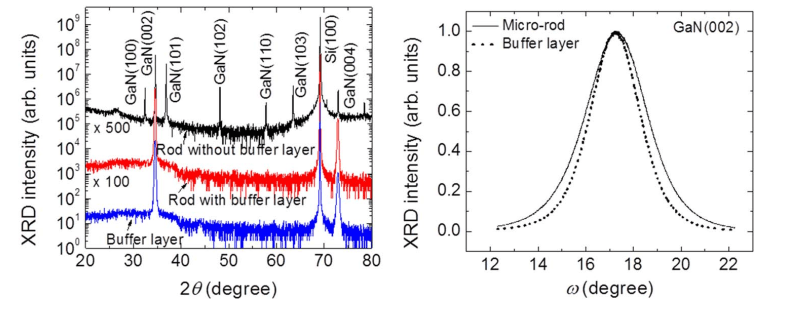
XRD
GaN micro-rods grown on graphene with/without a GaN buffer layer are examined using an XRD θ-2θ scan[8]. The range of scan was 20o-80o.
GaN with a buffer layer – Two Wurtzite Peaks
GaN with no buffer layer – Multiple Peaks
SEM
The FE-SEM image reveals the surface morphology of the GaN buffer layer and GaN micro-rods which is as expected[8].

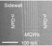
TEM
TEM images of the sidewall Multi-Quantum Well(MQW)(shown below) of the GaN micro-rod LEDs indicate growth comparable to baseline substrates like Sapphire/SiC[8].
- Electrical Characterization
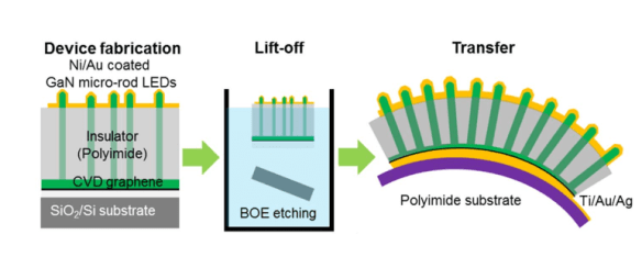
As the main objective of GaN growth on graphene is for flexible display applications, let us try to understand the electrical/optical output. Before doing the measurements, devices need to be fabricated on the grown films
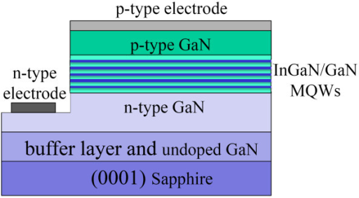
Device Fabrication[8]
- Post GaN micro-rod LED growth, the cavity between LEDs is filled using an insulating layer – polyimide
- The top layer of GaN micro-rod LEDs is opened using oxygen plasma etching
- Ni/Au used to make ohmic contact with p-GaN
- SiO2/Si substrate removed using wet(BOE) etching
- A Ti/Au is deposited and Ag is added at the bottom of LEDs to provide a reliable end for the current injection
- Coaxial GaN micro-rod LEDs were then transferred onto a polyimide substrate
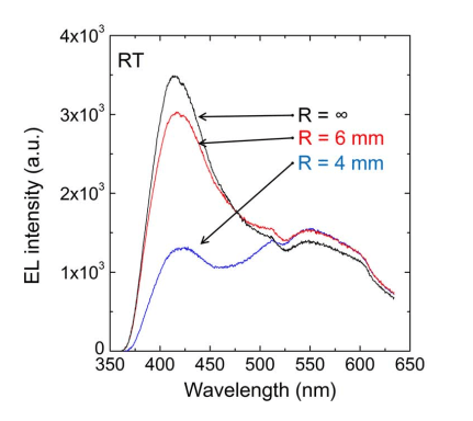
The emitted light from the fabricated LED despite the transfer process demonstrated reliable operation.

This operation continued even when the polyimide substrate was bent to change the radius of curvature. A radius of curvature of 6 mm for a 20-mm wide substrate under deformation(bent) does not cause the EL intensity & EL peak wavelength to change over 1000 cycles[8].
The methodology adopted by SNU researchers has the potential to integrate inorganic substrates with organic materials for future flexible displays. The requirement for a low thermal budget is accomplished by the introduction of a transfer technique.
B] Research at the University of Tokyo[2017]
A different approach was used by a research group at the University of Tokyo. Pulsed Sputtering Deposition(PSD) is used for III-Nitride film growth on glass using graphene as a buffer layer. In this technique, there is no transfer involved post-growth of GaN film[2].
- Graphene Growth
Graphene is grown on Ni sheets by Chemical Vapor Deposition(CVD) and subsequently transferred onto thermally oxidized SiO2 on Si substrates.
- GaN Growth
- Flexible substrates like glass, and plastic are amorphous in nature. For GaN growth on a glass substrate, a crystalline buffer layer should be introduced between GaN and glass
- PSD used for deposition enhances surface migration of the precursors thereby reducing the epitaxial growth temperature. The maximum temperature needed by PSD is 480oC in contrast to MOCVD for the growth of GaN[2]
- Material Characterization
SEM
The films grown by PSD were characterized using scanning electron microscopy (SEM)[2]. For comparative study, two sets of films were grown
GaN film grown on SiO2/Si – Rough Surface, small grains & size of several 100 nm
GaN film grown on Graphene Buffer/SiO2/Si – Smooth Surface

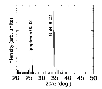
XRD
The GaN film using a graphene buffer layer was scanned using an XRD 2θ/ω plot. Diffraction peaks around 26.5o & 34.5o originate from graphene {0002} and GaN {0002}[2].
This shows that the crystal quality of the GaN film is improved by introducing the graphene buffer layer.
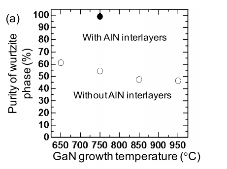
The GaN film grown using PSD consists of wurtzite and zincblende phases when grown on graphene at 750oC. Wurtzite Phase versus growth temperature is plotted for the GaN films[2].
Aluminum Nitride(AlN) interlayer/reaction blocking layer before GaN growth on graphene to ward off an interfacial reaction between GaN and graphene.
- Electrical Characterization
Material characterization for GaN film growth on graphene buffer will be followed by electrical characterization. Before doing the measurements, devices need to be fabricated on the grown films
Device Fabrication[2]
- AlN/graphene/amorphous SiO2 was the base structure
- n-type GaN layers were grown on the AlN interlayers
- Multiple quantum wells (MQWs) of InGaN/GaN and Mg-doped p-type GaN layers were grown on top
- Deposition of Pd/Au and In electrodes as ohmic contacts on the p- and n-type GaN surfaces

Electroluminescence (EL) measurements of the fabricated devices measured with various injection currents (2.1-10.8 mA)[2]. Blue/red LED’s grown by varying the Indium proportion were also characterized.

Conclusion
Considering the process flow, characterization, and reliability, III-Nitride semiconductors are a material of choice for displays, lighting, etc. Taking this point logically ahead, research groups and industry are trying to extend III-Nitride use in low thermal budget scenarios ie. III-Nitride on a low-cost substrate.
In this article, both the research groups have used graphene to grow GaN. LEDs made from GaN on graphene are comparable to those grown on Sapphire or SiC.
Innovative approaches can help to achieve the temperature requirement by permitting the usage of low-cost large-area substrates like glass. Pulsed Sputter Deposition(PSD) is an adapted sputter technique that is innovative and can be scaled up without any additional cost.
The next challenge will be to bring in polymeric substrates like plastic etc. These materials also support roll-to-roll processing & manufacturing like glass.
If you want to share your opinion kindly do so in the comments section or email me at u2d2tech@gmail.com.
References:
- https://publishing.aip.org/publishing/journal-highlights/bendy-leds
- J. Ohta et. al., “GaN-Based Light-Emitting Diodes with Graphene Buffers for Their Application to Large-Area Flexible Devices”, IEICE TRANS. ELECTRON., VOL.E100–C, NO.2 February 2017
- https://www.nature.com/articles/am2017118
- https://www.oled-info.com/flexible-oled
- M. Aleksandrova, “Specifics and Challenges to Flexible Organic Light-Emitting Devices”, Article ID 4081697, 8 pages, Advances in Materials Science and Engineering, Volume 2016
- L. Lin et. al., “Advances and challenges for flexible energy storage and conversion devices and systems “, Energy Environ. Sci., 7, 2101, 2014,
- S. Kim et. al., “Low-Power Flexible Organic Light-Emitting Diode Display Device“, Adv. Mater., 23, 3511–3516, 2011
- K. Chung et. al., “Growth and characterizations of GaN micro-rods on graphene films for flexible light emitting diodes”, APL Materials 2, 092512, 2014
- https://en.wikipedia.org/wiki/Graphene#Definition
- http://graphita.bo.imm.cnr.it/graphita2011/graphene.html
http://www.ledjournal.com/main/news/sapphire-substrate-continues-to-dominate-led-market/
- https://www.led-professional.com/resources-1/articles/high-quality-gan-substrates-for-modern-led-technology
- https://www.nature.com/articles/s41598-017-11757-1
- https://www.nature.com/articles/am2017118
K. Chung, C.-H. Lee, and G.-C. Yi, Science 330, 655,2010
- Y. Kobayashi, K. Kumakura, T. Akasaka, and T. Makimoto, Nature (London) 484, 223,2012
- C.-H. Lee, Y.-J. Kim, Y. J. Hong, S.-R. Jeon, S. Bae, B. H. Hong, and G.-C. Yi, Adv. Mater. 23, 4614, 2011
- http://www.appliedmaterials.com/en-in/node/3344641
P. Elmlinger et. al, “A Miniaturized UV-LED Based Optical Gas Sensor Utilizing Silica Waveguides for the Measurement of Nitrogen Dioxide and Sulphur Dioxide”, Proceedings 2017, 1(4), 55
S. Beck et.al, “Evaluating UV-C LED disinfection performance and investigating potential dual-wavelength synergy”, Volume 109, Pages 207-216, 2017
- http://www.ledsmagazine.com/articles/2016/02/nikkiso-delivers-50-mw-deep-uv-leds-with-10-000-hour-lifetime.html

Hi Shahaji,
Thanks for your feedback. Accordingly will cover that also.
LikeLike
Very nice article. Please also put on light on sensor applications
LikeLike
When I originally commented I clicked the -Notify me when new comments are added- checkbox and now every time a comment is added I get 4 emails with the identical comment. Is there any means you’ll be able to remove me from that service? Thanks!
LikeLike
This is really interesting, You’re a very skilled blogger. I have joined your rss feed and look forward to seeking more of your great post. Also, I’ve shared your site in my social networks!
LikeLike
I love the efforts you have put in this, appreciate it for all the great articles.
LikeLike
Unequivocally, a prompt reply 🙂
LikeLike
Great post, I believe people should learn a lot from this weblog its very user pleasant.
LikeLike
Thank you Newton
LikeLike
Hey there! I know this is somewhat off topic but I was wondering if you knew where I could get a captcha plugin for my comment form? I’m using the same blog platform as yours and I’m having difficulty finding one? Thanks a lot!
LikeLike
I just want to mention I am just newbie to blogging and honestly enjoyed your web-site. Likely I’m likely to bookmark your site . You surely come with superb posts. Kudos for revealing your blog site.
LikeLike
Thank you Enda
LikeLike
2019年春夏新作商品は販売!
■最新の2019年のブランドの新しいコピーを販売しています。
100%の品質保証を■!満足は保証! 100パーセントの顧客導入率!
■優れた品質と低価格、本物より!
■送料は無料です!買うために安心してください!
私たちの製品が良好であることを絶対的に自信を持って。
高品質低価格保証救助
製品の数、良い品質、低価格、多様う!
動作原理:品質、密着性も宅配、評判に焦点が最初に私たちのポリシーです。
偽物ブランド https://www.watcher0769.com/watch/menu-pid-30.html
LikeLike
I love visiting the Philippines. Korea does not have as many beautiful islands as you do. I’m comingbn back again this summer
LikeLike
【超人気質屋 】超美品、高品質、 N級 独占的な販売
★オメガ ブランドコピー最高等級時計大量入荷!
▽◆▽世界の一流ブランド品N級の専門ショップ ★
注文特恵中-新作入荷!-価格比較.送料無料!
◆主要取扱商品 バッグ、財布、腕時計、ベルト!
◆全国送料一律無料
◆オークション、楽天オークション、売店、卸売りと小売りの第一選択のブランドの店。
■信用第一、良い品質、低価格は 私達の勝ち残りの切り札です。
◆ 当社の商品は絶対の自信が御座います。
おすすめ人気ブランド腕時計, 最高等級時計大量入荷!
◆N品質シリアル付きも有り 付属品完備!
☆★☆━━━━━━━━━━━━━━━━━━━☆★☆
以上 宜しくお願い致します。(^0^)
広大な客を歓迎して買います!── (*^-^*)
■ホームページ上でのご注文は24時間受け付けております
LikeLiked by 1 person
I am only writing to let you be aware of what a fine discovery my friend’s girl enjoyed using your blog. She noticed several details, which include what it’s like to have a very effective teaching mindset to make certain people easily master chosen tricky issues. You really surpassed our expected results. Many thanks for giving the effective, safe, edifying and also easy thoughts on the topic to Evelyn.
LikeLiked by 1 person
Thank you for expressing this information during this awesome web site. i am going to write about this post on my fb account for my pals comanda mancare Buftea.
LikeLike
I can’t wait to visit Korea once this COVID-19 lockdown is lifted and we’re allowed to travel again
LikeLike
I think this is among the most significant information for me.
And i’m glad reading your article. But want to remark on some general things, The
web site style is perfect, the articles is really excellent : D.
Good job, cheers
LikeLike