Introduction
As demand for artificial intelligence (AI), high-performance computing, and advanced electronics grows, semiconductor companies are reaching the limits of traditional chip design.
Simply making transistors smaller is no longer enough.
The industry is now moving towards 3D chip architectures, where multiple semiconductor layers are stacked together.
A key technology enabling this transition is Through-Silicon Via (TSV) – a method that creates vertical electrical connections through silicon wafers, allowing chips to communicate faster while consuming less power.
What is Through-Silicon Via (TSV)?
Through-Silicon Via(TSV) is a semiconductor packaging technology where microscopic holes are drilled through a silicon wafer and filled with conductive materials, usually copper, to create vertical electrical pathways.
Earlier chip designs relied on side-by-side connections using traditional wire bonding.
TSV enables chips to be stacked vertically, reducing the distance signals need to travel and improving performance.
The biggest current application of TSV is High Bandwidth Memory (HBM) used in AI processors.
HBM stacks multiple memory layers connected through thousands of TSVs, enabling extremely high data transfer rates required by AI models.
Modern HBM3E memory can deliver bandwidth approaching 1 TB/s per stack, while advanced AI systems combine multiple HBM stacks to achieve several terabytes per second of memory bandwidth.
How is TSV Technology Implemented?
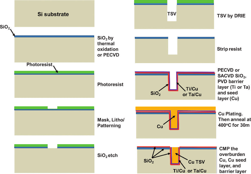
The TSV manufacturing process involves several precision steps:
1) Creating microscopic vias:
Tiny vertical holes are etched through silicon wafers, typically using deep reactive ion etching technology. These vias can range from a few micrometres in diameter depending on the application. Advanced TSV designs commonly use via sizes between 5-10 micrometres.
2) Filling with conductive material:
The vias are insulated and filled with copper to create electrical connections between chip layers.
3) Stacking and bonding chips:
Multiple semiconductor dies are aligned and bonded together using techniques such as wafer bonding and hybrid bonding.
4) Testing and packaging:
The stacked structure undergoes extensive testing because even a small defect can impact the performance of the entire package.
Where is TSV Technology Used?
TSV adoption is expanding across multiple industries:
A] Artificial Intelligence and Data Centres:
AI accelerators depend on TSV-based HBM because traditional memory cannot provide sufficient bandwidth. Each HBM stack can contain thousands of TSV connections, enabling faster communication between memory and processors.
B] Consumer Electronics:
Smartphone camera sensors, advanced processors, and compact electronics use TSV to reduce size and improve performance.
C] High-Performance Computing:
Supercomputers and scientific computing platforms use 3D packaging to achieve higher computing density.
D] Automotive and Sensors:
Autonomous vehicles, industrial sensors, and MEMS devices use TSV for compact and reliable electronic integration.
Challenges in TSV Adoption
Despite its advantages, TSV manufacturing remains complex and expensive.
Major challenges include
a) Manufacturing yield – HBM production requires precise stacking of multiple layers, and defects in TSV formation or copper filling can reduce output.
b) Thermal management is another challenge. Stacking chips increases computing density but also makes heat removal more difficult.
c) Cost is also a concern. Advanced packaging requires specialised equipment and processes, contributing significantly to semiconductor manufacturing expenses.
The Future of TSV: Enabling the Next Generation of Computing
The TSV market is expected to grow rapidly as AI and advanced computing expand.
Industry estimates suggest the global TSV technology market could grow from around $3-4 billion in 2025-26 to over $20 billion by 2035, driven largely by AI accelerators, HBM, and chiplet-based architectures.
Future developments will focus on:
- Higher-density chip stacking
- Smaller TSV structures
- Improved thermal management
- Hybrid bonding technologies
- Integration of logic, memory, and specialised accelerators in a single package
The semiconductor industry is moving from a two-dimensional world of smaller chips towards a three-dimensional world of interconnected chip systems. TSV is one of the foundational technologies making this transformation possible.
References for Further Reading
- TrendForce – High Bandwidth Memory and TSV market analysis
https://www.trendforce.com/ - Global Market Insights – Through-Silicon Via Technology Market Forecast
https://www.gminsights.com/ - DataM Intelligence – TSV Technology Market Outlook and AI Applications
https://www.datamintelligence.com/


Leave a Reply